How Do Transistors Work? The Building Blocks of Modern Computing
4 min read
You've probably heard of transistors. They're the fundamental elements that computers are built from. They can be shrunk to a few nanometers; the switch from vacuum tubes to transistors drove the information revolution, and Moore's law famously predicts that the number of transistors in a computer chip doubles every two years.
But what actually are transistors? How do they work? How are complex computers built up from them?
Diodes
We'll start by understanding how diodes work. You'll see how this relates to transistors in a moment.
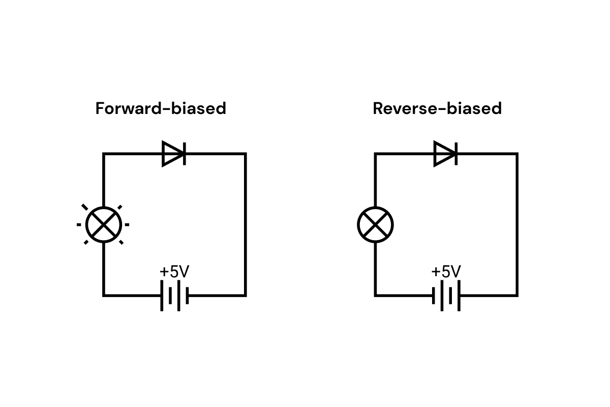
Diodes are elements that only allow current to flow one way in a circuit. In the diagram below, the diode in the left circuit is "forward-biased", so current flows and the lightbulb lights up. The diode in the right circuit is "reverse-biased", so no current flows and the lightbulb remains unlit.
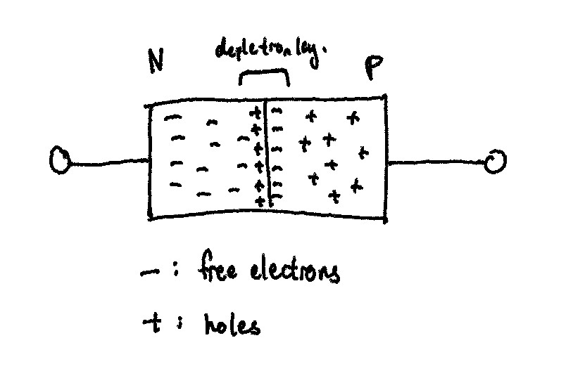
Diodes function using something called the "PN junction." P and N refer to two types of silicon semiconductor material.
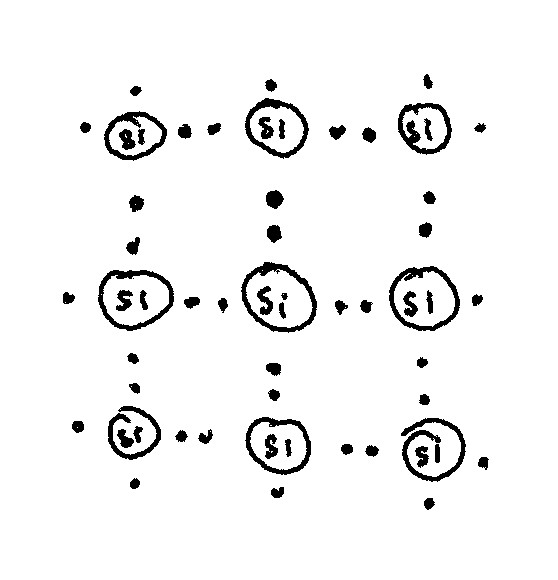
On its own, silicon has four valence electrons. In a crystal lattice, silicon forms stable bonds with four other silicon atoms around it. There are no free electrons and thus no conductivity of electricity.
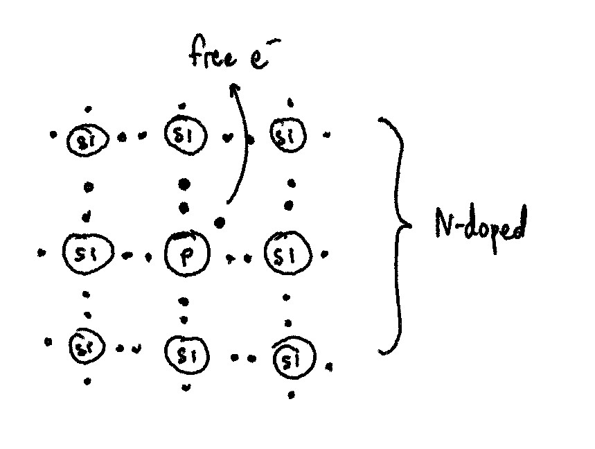
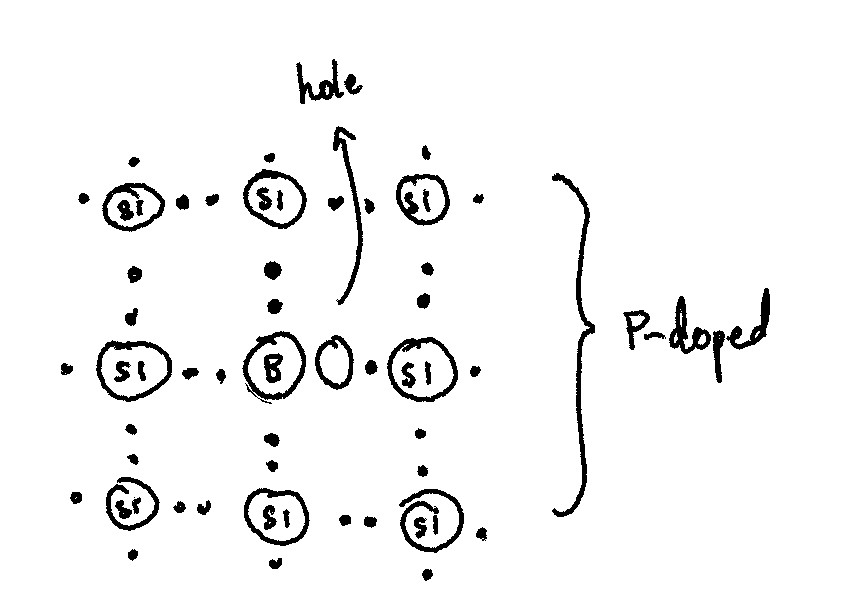
To make silicon useful, we have to inject another kind of atom to allow for free electron flow. This injection is referred to as either "N-doping" or "P-doping".
In N-doping, an atom with five electrons, such as phosphorous, is injected. Four of these electrons form stable bonds with surrounding silicon atoms, but the fifth electron is now free to move around the lattice.
In P-doping, an atom with three electrons, such as boron, is injected. The three electrons form bonds with surrounding silicon atoms, but now there is a "hole" to which other electrons can move to fill.
In a diode, N-doped and P-doped silicon are stacked next to each other. The free electrons in the N-doped silicon are attracted to the holes in the P-doped silicon, and start moving across the divide. When they cross the divide, they fill the holes in the P side. Now there's a negative charge on the P side of the divide, and electrons from the N side are repelled from rather than attracted to the P side. Thus, electrons stop flowing to the P side, and at equilibrium a depletion layer is formed with a potential difference of 0.7 V.
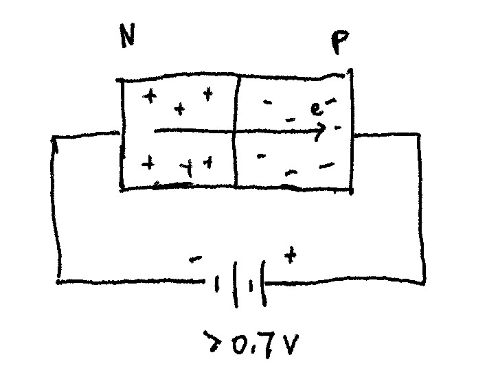
When a voltage of greater than 0.7 V is applied across the diode, the potential difference of the depletion layer is overcome, and electrons are able to make the jump from the N to the P side, completing the circuit and creating a current.
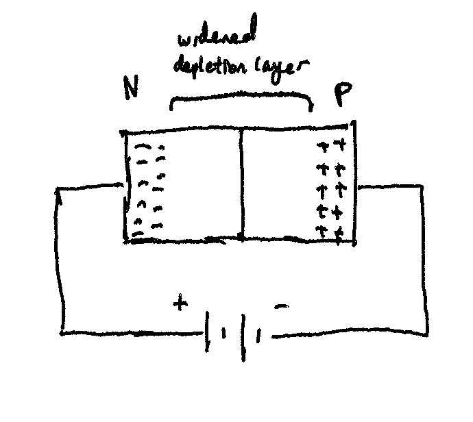
When a voltage of the opposite direction is applied, the depletion layer widens: electrons on the N side are attracted to the positive terminal of the voltage source, and holes on the P side to the negative terminal. Thus, there is no electron flow and no current.
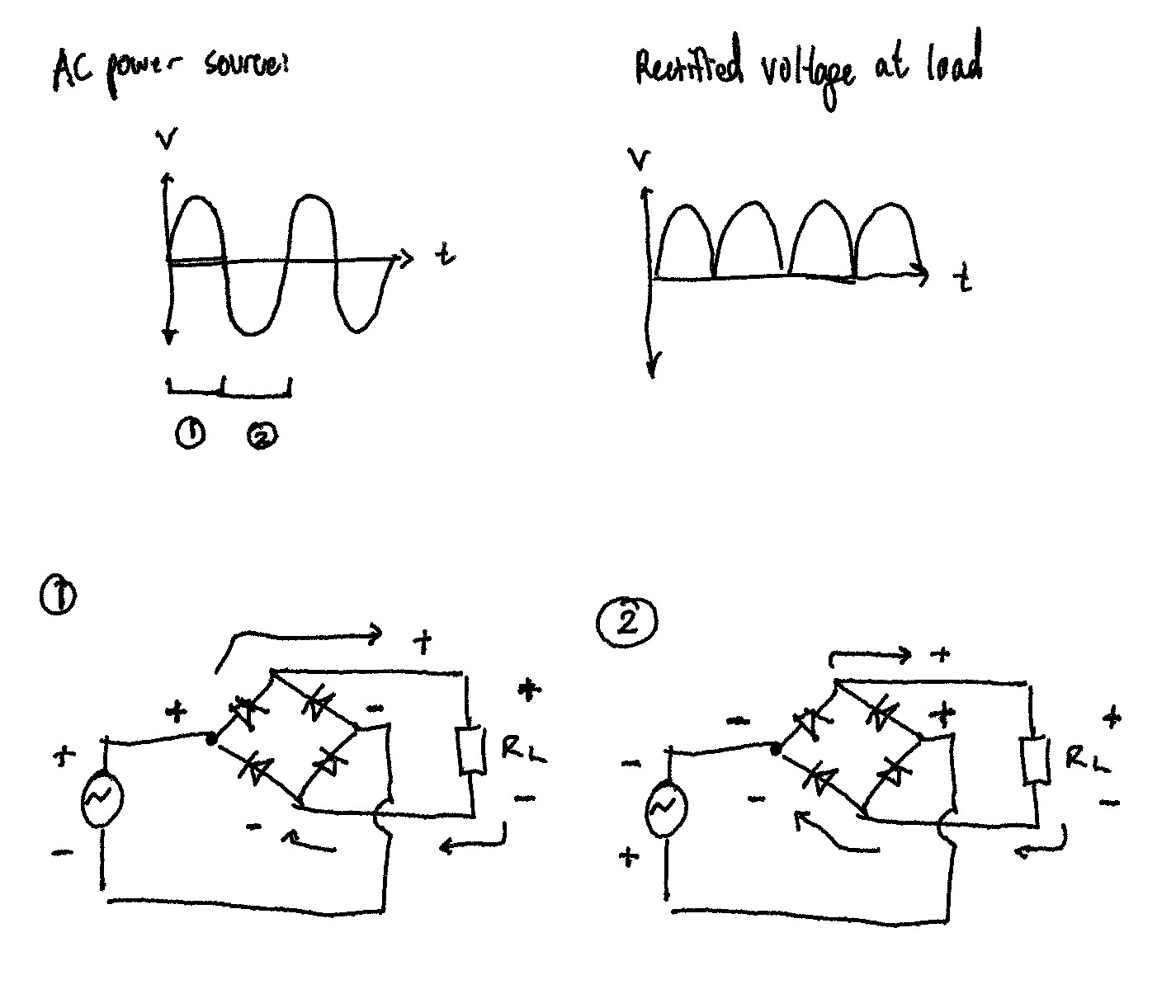
Diodes are useful for a variety of purposes, such as rectifying AC to DC power:
Bipolar Junction Transistor
We're now ready to talk about transistors! The first of two types of transistors we'll talk about is the bipolar junction transistor, invented by William Shockley at Bell Labs in 1948 (who would win the 1956 Nobel Prize in Physics for his research on semiconductors and transistors, along with two other Bell Labs researchers).
A BJT consists of N, P, and another N layer being stacked back-to-back against each other.
When a voltage is applied on the two terminal N layers of the transistor either way, no current flows.
The magic happens when we introduce a second loop of the circuit, connecting one N terminal to the P layer in the middle. Looking at this loop in isolation, we see that it's just the diode circuit we were looking at earlier!
When a forward-biased voltage of greater than 0.7 V is applied in this diode circuit, current flows across the NP junction and completes the top loop of the circuit. Overcoming the depletion layer of the NP junction also closes the bottom loop of the circuit and allows current to flow.
Thus, we see that our transistor is functioning as a switch! When a sufficient voltage, i.e. > 0.7 V, is applied in the top loop of the circuit, the bottom loop is closed. When the voltage is insufficient, the bottom loop is open. Transistors can be much smaller and faster than physical switches, which is what makes them useful for computer chips that cram billions of transistors into a small slab of silicon.
Bipolar junction transistors can also function as amplifiers. An electric signal in the top loop, for example a microphone that introduces voltage fluctuations corresponding to air pressure differences, is reflected in the bottom loop as well. With a larger voltage source in the bottom loop, this signal is thus amplified, and can, for example, now drive a speaker to amplify sound from the microphone.
In a BJT, the three contacts are called the emitter, base, and collector. You can buy a whole tray of transistors for a few dollars, and they're commonly used in hobby electronics projects.
Field Effect Transistor
For computer chips, though, BJTs are still too bulky. Another kind of transistor, the field effect transistor (FET), are a later development and actually used in integrated circuits and computer chips.
FETs look a little different from BJTs:
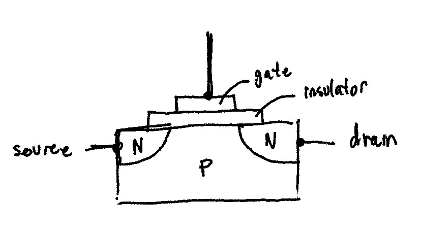
Our N and P layers are still present, along with two terminals attached to each of the N layers. Instead of a second loop connected directly to the P layer, though, the third terminal of a FET is the "gate", prevented from contacting the N or P layers directly by an insulator.
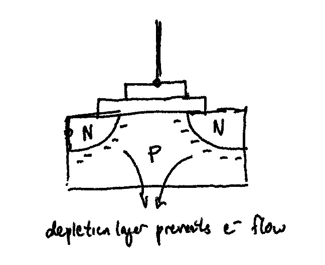
As before, a depletion layer is formed between the N and P layers. When a voltage is applied across the two N terminals, no current is able to flow.
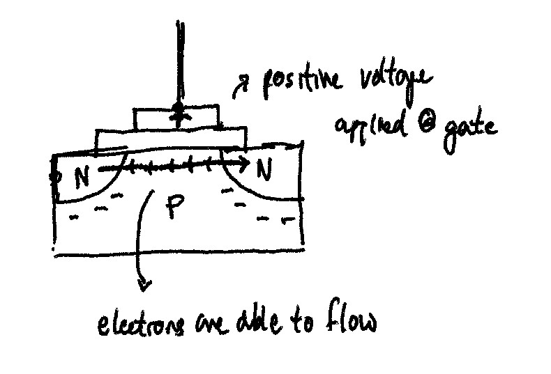
When a positive voltage is applied to the gate, the field created eliminates the depletion layer in a region between the two N terminals, allowing electrons to flow and closing the circuit. Thus, as before, the FET functions as a switch.
A particular type of FET, metal-oxide-semiconductor field-effect transistors, or MOSFETs, are credited with revolutionizing the electronics industry and kicking off the age of modern computing. Invented by Mohamed Atalla and Dawon Kahng at Bell Labs in 1959, MOSFETs have since become the most frequently manufactured device in history, with 13 sextillion -- that's 13e21 -- manufactured to date.
To see concretely how transistors are used in computers, consider basic logic gates like AND and OR. From these gates, all components of a computer system -- memory, storage, processing -- can be built. In turn, logic gates can be constructed out of basic transistor circuits:
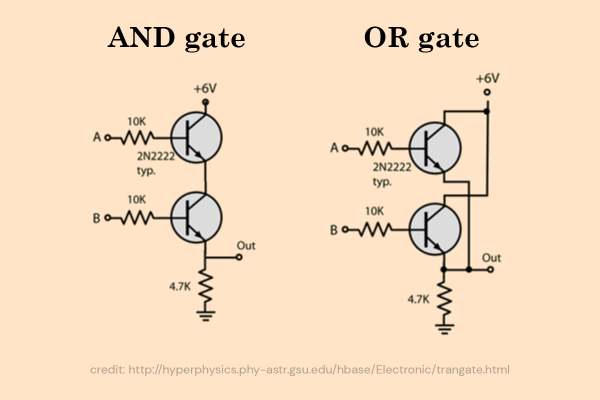
Thus, with FETs, millions and billions of logic gates can be crammed onto IC chips, memory modules, solid-state storage devices, and more, powering the electronics around us.
Contact me
Have a question about my work? Want to work together? Don't hesitate to reach out!
Email me at hello@samsonzhang.com, or message me on Twitter @wwsalmon.